Ready
Design Journey
The journey of a thousand miles begins with the first step. When we set out to design the S0 gateway board, we had a clear vision: create a comprehensive solution for aggregating smart meter data from both wireless and wired M-Bus meters. What followed was an educational journey through PCB design challenges, debugging sessions, and valuable lessons that shaped not just our board, but our approach to hardware design.

The Vision
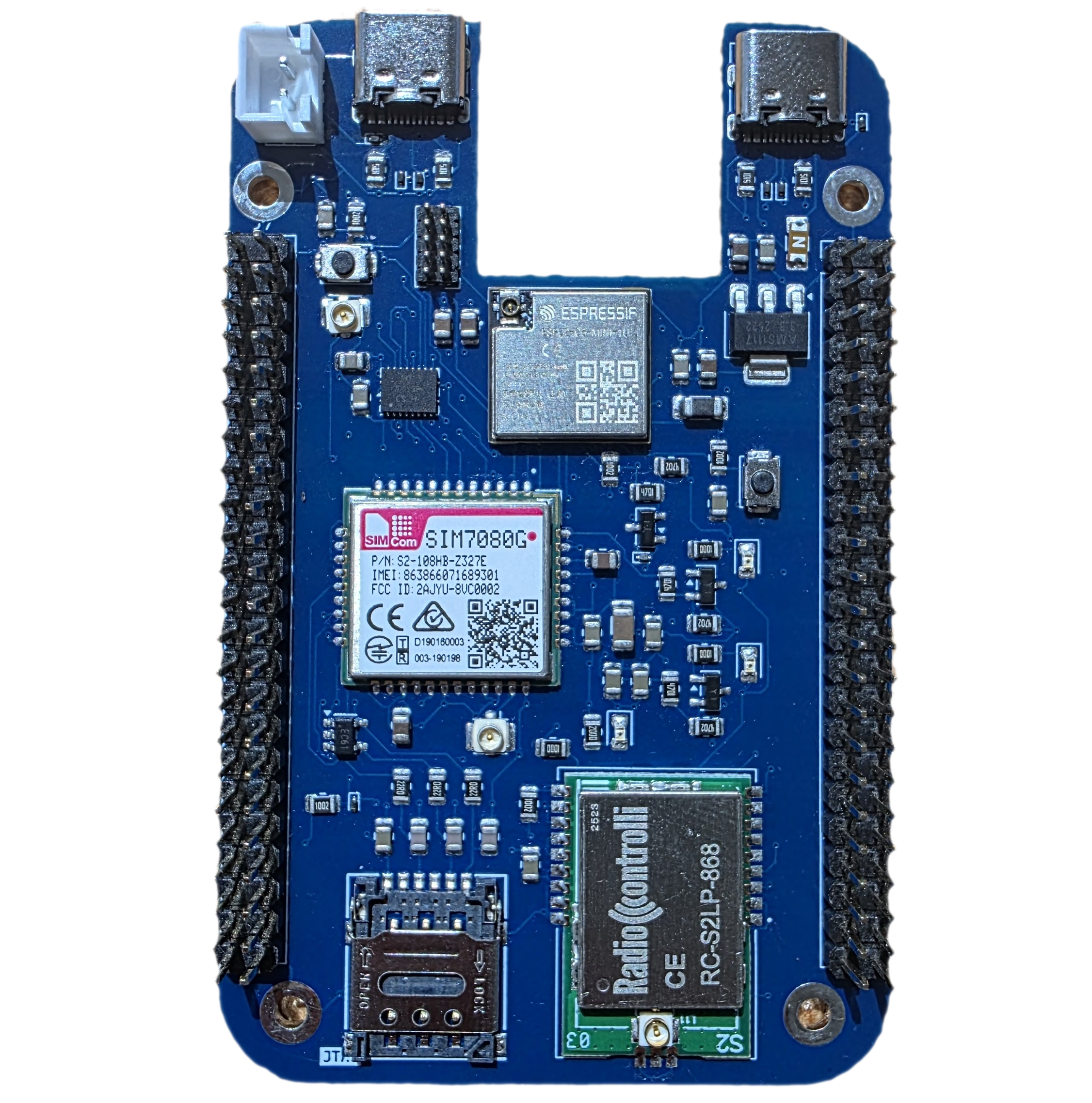
The S0 is a dual-board system designed to act as a smart meter gateway with impressive connectivity options:
The S0 Main Board features:
- ESP32-C6 microcontroller (RISC-V powered, USB-C programmable)
- SIM7080G NB-IoT module for cellular connectivity
- RC-S2LP Wireless M-Bus module (868MHz) for reading wireless meters
- Battery power support via JST connector
- JTAG debugging capability
The S0 Baseboard extends functionality with:
- W5500 Ethernet chip with RJ45 Jack and Magnetics
- TSS721ADR Wired M-Bus module for reading wired meters
- SD card slot for local data logging
- Power management and distribution
Both boards connect via 92-pin headers, creating a compact yet powerful gateway system. Our ambitious goal for S0? Make it pin-compatible with the BeagleV-Fire development board.
Just like any design, we had our fair share of challenges, which has made this journey a learning experience.
Challenge 1: The Form Factor Puzzle
Our first major hurdle hit us during component placement. We wanted the S0 to be pin-to-pin compatible with the BeagleV-Fire while maintaining a compact form factor. It sounds simple on paper, but when you’re trying to fit multiple radio modules, power circuits, and connectors onto a constrained PCB while maintaining proper spacing for RF performance, reality sets in quickly.
The ESP32C6, SIM7080G, and RC-S2LP modules each had their own keep-out zones and antenna requirements. We found ourselves playing 3D Tetris, rotating components, trying different orientations, and constantly checking clearances. The lesson? Start with your largest and most constrained components first, then build around them. And always, always verify mechanical compatibility early in the design phase.
Challenge 2: The Impedance Matching Reality
Routing the Baseboard introduced us to the critical world of impedance matching. We knew differential pairs needed careful routing, but understanding it theoretically and implementing it practically are two different things.
The Ethernet circuit with the W5500 was particularly demanding. Those differential pairs needed 100Ω impedance matching, which meant calculating trace widths, spacing, and considering the PCB stackup. Get it wrong, and you get signal reflections, communication errors, and mysterious failures.
What we learned: Use your PCB manufacturer’s stackup calculator. Don’t guess at trace widths for controlled impedance. And yes, all those differential signals — USB, Ethernet, high-speed SPI — they all need proper impedance matching for reliable communication.
Challenge 3: The SPI Bus Sharing Saga
This one caught us off guard. We designed the Baseboard with both the Ethernet chip and SD card sharing the SPI bus — a common and reasonable approach. Different chip selects would handle arbitration, right?
Wrong.
We discovered that our SD card was holding the MISO line even after being deselected. This meant the Ethernet chip couldn’t communicate properly because the SD card was still driving the shared bus. Classic bus contention.

The solution: We implemented a tri-state buffer (essentially an SPI isolator) on the SD card’s MISO line. The buffer’s enable pin connects to the SD card’s chip select, ensuring that when the SD card is deselected, it truly releases the MISO line. Problem solved, and we gained a deeper understanding of proper SPI bus sharing techniques.
Challenge 4: The Bootstrap Pin Blunder
This was a facepalm moment. On the first revision of the S0, we connected SPI lines to the ESP32-C6’s bootstrapping pins. For those unfamiliar, bootstrap pins are sampled during power-up to determine boot mode and configuration.
The result? A completely non-functional SPI bus. The ESP32-C6 was fighting with our peripherals for control of those pins during startup.
The fix: We moved the SPI connections to regular GPIO pins in Rev2. The lesson: Always check your microcontroller’s datasheet for special-purpose pins, especially bootstrap, strapping, and configuration pins. Don’t assume any GPIO is fair game.
Challenge 5: SPI vs. SD Card Pin Mapping
Here’s a subtle one that cost us some debugging time. We thought we had correctly connected the SD card to the SPI bus on the Baseboard. The pinout looked right, the connections were there, but nothing worked. The issue? SPI domain and SD card domain use different pin naming conventions and mapping. What’s MOSI in SPI world isn’t necessarily CMD in SD card world without proper mapping. We had made assumptions about pin compatibility without verifying the actual protocol requirements.

The takeaway: Don’t rely on “looks right” when dealing with protocol conversions. Verify with datasheets, reference designs, and if possible, official application notes. SPI-to-SD interfacing has specific requirements that must be met.
Challenge 6: The Power Circuit Journey
This challenge taught us perhaps the most important lesson of the entire project. On the Baseboard, we designed what we thought was a clever overvoltage protection circuit using a MOSFET. We were proud of the design — it was elegant, compact, and theoretically sound.
It didn’t work. The MOSFET wouldn’t turn on, and the board wouldn’t power up.

We spent hours debugging, checking gate voltages, trying different MOSFETs, questioning our understanding of transistor physics. Then it hit us: we never simulated this circuit before committing to the PCB.
This realization led to a broader epiphany. We had multiple ideas for complex power protection schemes. Some were innovative, some were borrowed from high-end designs. But complexity for complexity’s sake is engineering ego, not engineering excellence.
The solution: We simplified. Dramatically.
Overvoltage protection: resistor-Zener diode clamp (simple, reliable, well-understood) Overcurrent protection: a fuse (can’t get simpler than that) Reverse polarity protection: Schottky diode (low drop, fast, effective) Not innovative. But it works, it’s reliable, and anyone debugging the board can understand it instantly.

The lesson: Simulate before you fabricate. And remember: a working simple circuit beats a broken clever one every single time. Your future self (and anyone else working on the project) will thank you for choosing clarity over complexity.
What We’d Do Differently
Looking back at this journey, here’s what we’d change:
- More upfront mechanical planning — Create a 3D model early with all components placed before starting routing
- Impedance calculator from day one — Don’t wait until routing to think about controlled impedance
- Bus sharing validation — Test SPI bus sharing scenarios on a breadboard first
- Pin assignment review — Have a dedicated review session for all microcontroller pin assignments checking for conflicts
- Reference design study — Spend more time with reference designs, especially for SD card interfaces and Ethernet W5500
- Circuit simulation mandatory — Make LTSpice simulation a requirement before any new circuit enters the schematic
- Simplicity first — Start with the simplest working solution, then optimize only if needed
The Win
Despite the challenges, Rev3 of the S0 system works. It reliably reads both wireless and wired M-Bus meters, communicates over NB-IoT, logs to SD card, and connects via Ethernet. The form factor works with the BeagleV-Fire. The power circuit is rock-solid.
More importantly, we learned lessons that will make every future design better. Hardware design is iterative, and every challenge is a chance to deepen understanding.
For Those Starting Their Journey
If you’re designing your first complex board, here’s our advice:
- Start simple — Get basic functionality working before adding features
- Read everything twice — Datasheets, app notes, reference designs — read them carefully
- Simulate critical circuits — Especially power, protection, and anything you haven’t built before
- Plan for debugging — Add test points, LED indicators, and JTAG/SWD access
- Embrace iteration — Rev1 rarely works perfectly, and that’s okay
- Document your mistakes — They’re learning opportunities, not failures
- Keep it simple — Especially for power and protection circuits
The S0 journey taught us that good hardware design isn’t about being clever — it’s about being thorough, methodical, and humble enough to learn from mistakes. Every challenge we faced made the final product better and made us better engineers.
Here’s to many more revisions, lessons learned, and working boards. 🔧